
Understanding LED Packaging Technologies: IMD, SMD, GOB, COB, COG, and More
- Tse Cherie
- Jun 28
- 12 min read

LED packaging technologies such as SMD, IMD, GOB, VOB, COB, COG, MIP, and CSP directly affect pixel pitch, durability, maintenance, image quality, and long-term reliability in modern LED display systems. For engineers, system integrators, procurement teams, distributors, and B2B buyers, understanding these differences is essential when selecting the right solution for a fine-pitch LED display, rental screen, commercial display, control room, or future-facing Mini LED or Micro LED project.
In simple terms, these technologies describe how LED chips are packaged, mounted, protected, and integrated into display modules. Some are mature and widely used in mainstream products, while others are more closely linked to high-end fine-pitch applications or the future development path of MLED. This article explains what these technologies mean, how they work, where they are used, and how to evaluate them in real-world LED display selection.
1. What Are Small-Pitch LED, Mini LED, Micro LED, and MLED?
Before comparing packaging technologies, it is important to define several closely related industry terms.
Small-pitch LED usually refers to LED displays with a pixel pitch between P1.0 and P2.0. These displays are designed for relatively short viewing distances and are widely used in meeting rooms, control rooms, studios, command centers, and premium indoor commercial applications.
Mini LED generally refers to LED chips in the 50–200 μm range, with display pixel pitch often in the 0.3 mm to 1.5 mm range. Mini LED sits between conventional fine-pitch LED and Micro LED in the broader technology roadmap.
Micro LED usually refers to LED chips smaller than 50 μm, with pixel pitch below 0.3 mm. This is the direction of ultra-fine-pitch direct-view displays and next-generation high-resolution display technologies.
MLED is the umbrella term that includes both Mini LED and Micro LED. In industry discussions, MLED is often used to describe the overall trend toward smaller chips, tighter pixel pitch, and more advanced packaging and transfer technologies.
A simple way to distinguish them is:
Small-pitch LED describes a pitch category
Mini LED and Micro LED describe chip-scale and display-evolution concepts
MLED groups Mini LED and Micro LED together
2. Why Does LED Packaging Matter in an LED Display System?
LED packaging plays a central role between the LED chip and the display module. It determines how RGB chips are electrically connected, arranged into pixels, mounted on a substrate, and protected from environmental or mechanical damage.
That makes packaging much more than a manufacturing detail. It directly affects:
pixel pitch capability
display flatness
impact resistance
dust and moisture protection
image consistency
heat dissipation
maintenance method
failure rate
service life
cost structure
Although packaging is different from the sending card, receiving card, video processor, driver IC, and control software, it influences how the full LED control system performs in practice.
For example:
SMD is still widely used because it is mature, economical, and easy to maintain.
GOB and VOB are often selected when stronger surface protection is needed.
COB is increasingly used in high-end fine-pitch LED displays where reliability and visual performance matter more.
COG is more relevant to future Micro LED development.
MIP has become important in discussions around advanced Mini LED and Micro LED manufacturing.
In short, packaging affects not only the pixel structure, but also the display’s practical performance in installation, operation, and long-term maintenance.
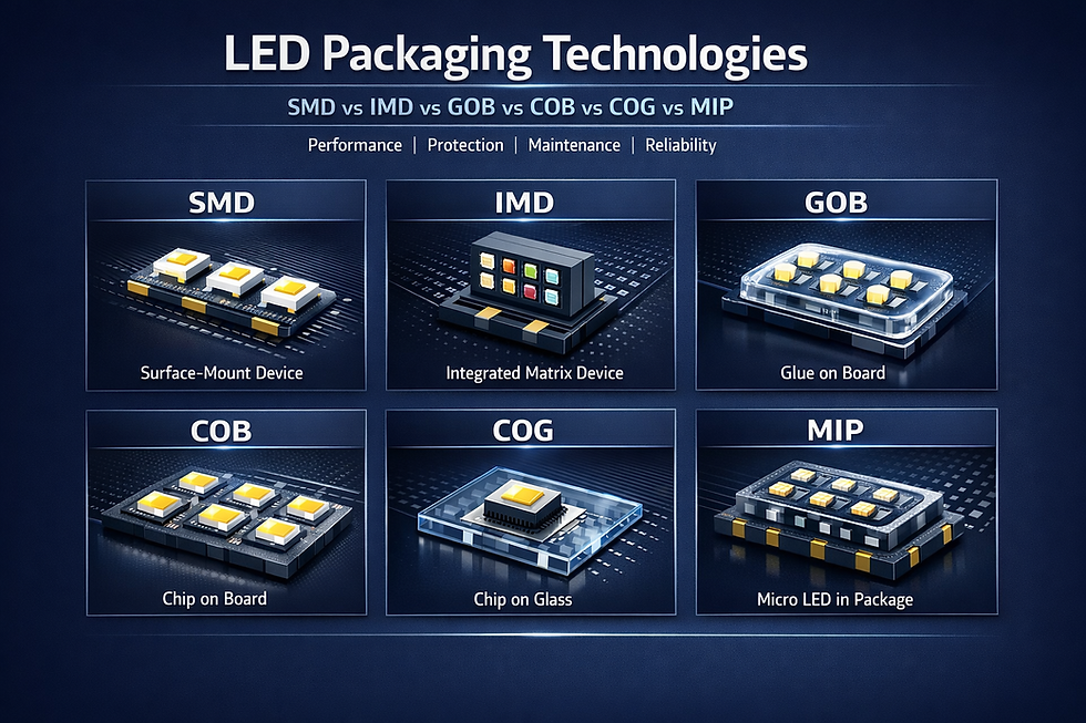
3. How Do LED Packaging Technologies Work?
At the most basic level, an LED display starts with red, green, and blue LED chips. These chips must be turned into usable display pixels. The way this happens depends on the packaging route.
Depending on the technology, the chips may be:
packaged individually and then mounted onto a PCB
integrated into a multi-in-one package
mounted directly onto PCB
mounted directly onto glass
packaged at chip scale
integrated into packaged pixel units before transfer
These pixel structures then become part of an LED module connected to:
driver ICs
PCB circuitry
receiving cards
cabinet communication links
sending cards
video processors
control software
This is why packaging matters beyond the component level. It affects display assembly, calibration, protection, maintenance, and system reliability.
It is also useful to distinguish between package structures and protective processes:
SMD, IMD, COB, COG, MIP, and CSP mainly describe packaging or integration structures
GOB and VOB mainly describe protective coating or encapsulation processes applied over the module surface
There is also a related distinction between front-mount chips and flip-chip structures.
A front-mount chip usually has the electrode and light-emitting surface on the same side and often relies on wire bonding.
A flip-chip places the electrode side downward, reducing or eliminating wire bonding.
Flip-chip structures can improve stability, reduce failure risk, and support smaller package sizes. This is one reason they are often discussed in relation to COB, CSP, Mini LED, and Micro LED.
Another related system consideration is the drive architecture:
Common anode is mature and cost-effective, but typically less energy-efficient.
Common cathode allows more precise voltage supply to RGB chips, helping reduce heat and power consumption.
While these are not packaging technologies in the strict sense, they are often evaluated together when selecting a display for demanding applications.
4. What Types of LED Packaging Technologies Are Available?
SMD
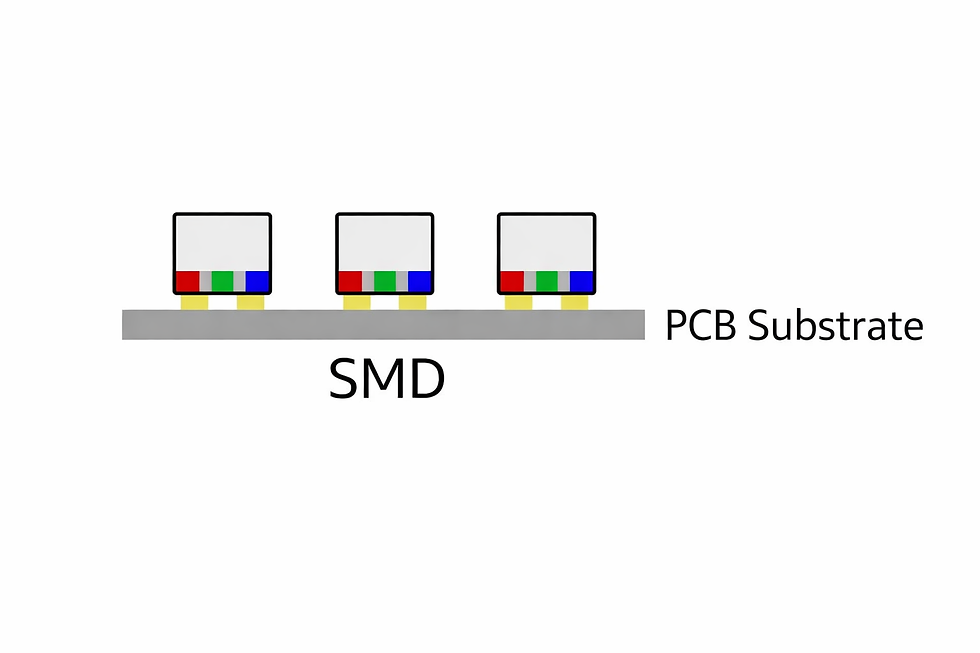
SMD (Surface Mounted Device) is the most established packaging technology in the LED display industry. In this method, the LED lamp bead is first packaged, then mounted onto a PCB using surface-mount technology and reflow soldering.
SMD remains mainstream because it offers:
mature manufacturing processes
a broad and stable supply chain
relatively low production cost
good thermal performance
straightforward maintenance
Its main limitation is that the lamp beads are relatively exposed, which can make the module more vulnerable to impact, moisture-related issues, and dead pixels in demanding environments.
IMD
IMD (Integrated Matrix Devices) is a matrix-style integrated packaging solution, often described as a multi-in-one format. A typical example is 2×2, or 4-in-1, where multiple RGB chip groups are integrated into one package.
IMD is often seen as a transition between traditional SMD and COB. It improves anti-collision performance and supports finer pitch, often around P0.7 and below in some applications.
One trade-off is that because multiple positions are integrated into one package, color consistency may require additional calibration.
GOB
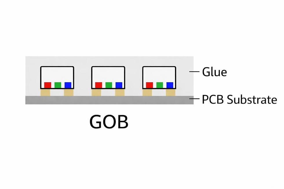
GOB (Glue On Board) is a protective encapsulation process applied over the LED module surface, most commonly on top of an SMD-based module. Transparent material is used to cover the board and package units, creating a protective layer.
GOB is mainly used to improve resistance to:
moisture
water
dust
impact
static electricity
salt spray
oxidation
vibration
This makes it useful in harsher environments and in applications where the display may be touched or transported frequently.
The trade-offs can include more difficult repair work, process sensitivity related to adhesive quality, and possible thermal or stress-management concerns.
VOB
VOB is generally considered a more refined version of GOB. It uses a thinner and more precisely controlled coating process to improve surface flatness, protection, and black consistency.
Compared with conventional GOB, VOB is often associated with:
thinner coating
stronger protection
lower failure rate
improved black consistency
higher contrast
softer visual appearance
easier maintenance
In practical product positioning, VOB is often presented as a higher-end protective solution for fine-pitch LED displays.
COB
COB (Chip on Board) means mounting LED chips directly onto the PCB substrate and then encapsulating them as an integrated surface. Instead of packaging each lamp bead separately, COB builds a more unified module structure.
Its practical advantages include:
stronger anti-collision performance
better anti-static protection
better dust and moisture resistance
smoother display surface
reduced moiré
smaller pitch potential
lower dead-pixel risk
Because of these strengths, COB is widely regarded as one of the key technical routes in the Mini LED era, especially for premium indoor fine-pitch applications.
COG
COG (Chip on Glass) means mounting LED chips directly onto a glass substrate rather than PCB.
This substrate difference is important because glass can support much finer structures, making COG highly relevant to Micro LED development. In theory, pixel pitch can go below P0.1.
COG is not the mainstream route for most current commercial LED display projects, but it is important in future ultra-fine-pitch display development.
MIP
MIP (Module in Package) is a multi-chip integrated packaging approach that has attracted growing attention in Mini LED and Micro LED development.
One of the major technical difficulties in Micro LED manufacturing is mass transfer. MIP helps address this by integrating RGB sub-pixels into packaged pixel units before transfer, reducing the complexity of moving a huge number of tiny chips individually.
For this reason, MIP is increasingly seen as an important route in advanced MLED manufacturing.
CSP
CSP (Chip Scale Package) is a chip-level package structure and can be viewed as a miniaturized evolution beyond traditional SMD. It is often associated with flip-chip packaging and significantly reduced package size, often close to 1.2 times the chip size.
Compared with SMD, CSP offers a smaller footprint. Compared with more complex integrated structures, it can also provide good chip consistency in some applications.
Its main challenge is that the smaller pad size and tighter tolerances require higher process precision, better equipment, and stricter manufacturing control.
5. Where Are These LED Packaging Technologies Commonly Used?
Different packaging technologies suit different application environments and performance requirements.
SMD
SMD is widely used in:
standard indoor LED displays
outdoor advertising screens
meeting room displays
commercial signage
many fixed installation projects
It remains a practical choice where cost control, mature supply, and easy maintenance are important.
IMD
IMD is commonly used in:
fine-pitch indoor LED displays
applications requiring better anti-collision performance
projects that need a balance between finer pitch and controlled cost
GOB and VOB
GOB and VOB are commonly used in:
rental LED displays
education environments
public spaces with touch risk
transport hubs
humid or dusty environments
Their value lies mainly in stronger front-surface protection.
COB
COB is especially suitable for:
control rooms
command centers
monitoring centers
studios
boardrooms
premium indoor display walls
These applications benefit from higher reliability, smoother visual appearance, and smaller pitch support.
COG
COG is more closely associated with:
advanced R&D
Micro LED development
future ultra-fine-pitch display products
MIP and CSP
MIP and CSP are more relevant to:
advanced Mini LED and Micro LED manufacturing
high-density display integration
next-generation fine-pitch display development
6. What Are the Main Advantages of These Technologies?
The progression from SMD to IMD, COB, COG, MIP, and CSP reflects the industry’s effort to improve performance while pushing pixel pitch smaller.
Common advantages across newer packaging routes
Compared with conventional structures, newer packaging technologies may offer:
finer pixel pitch
better front-surface protection
lower failure rates
stronger environmental resistance
improved visual consistency
better close-viewing performance
better suitability for Mini LED and Micro LED trends
Technology-specific strengths
Each route has its own value:
SMD: mature, economical, easy to maintain
IMD: more integrated than SMD, with better anti-collision performance
GOB: stronger protection for exposed module surfaces
VOB: thinner and more uniform protective coating
COB: high reliability, reduced moiré, integrated display surface
COG: extremely fine pitch potential
MIP: reduced mass-transfer complexity in advanced MLED manufacturing
CSP: compact structure and miniaturization potential
For practical LED display projects, the biggest advantage is not novelty by itself. It is the ability to align packaging structure with real application needs.
7. What Are the Limitations of These LED Packaging Technologies?
No packaging technology is universally ideal. Each has trade-offs that should be evaluated in the context of the project.
SMD limitations
exposed lamp beads
weaker impact resistance
lower protection in harsh environments
IMD limitations
color consistency may need closer calibration
process control becomes more important as pitch decreases
GOB limitations
more difficult repair work
adhesive quality is critical
thermal and stress management need attention
VOB limitations
performance depends heavily on coating precision
process quality has a strong effect on final consistency
COB limitations
higher process complexity
may increase cost in some projects
maintenance expectations differ from traditional SMD products
COG limitations
still more future-oriented than mainstream in many current projects
ecosystem maturity is lower than standard commercial solutions
MIP limitations
adoption is growing, but the ecosystem is still developing
upstream process capability remains critical
CSP limitations
higher manufacturing precision requirements
tighter process and equipment tolerances
For buyers and system integrators, the key point is that packaging should be selected based on application fit, not just technical buzzwords.
8. How Should You Choose the Right LED Packaging Technology?
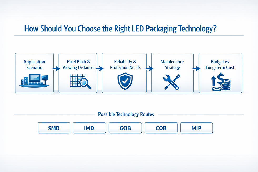
A good selection process should consider technical fit, maintenance strategy, and purchasing realities at the same time.
1) Start with the application
Ask where the display will be used:
control room
retail space
conference room
rental stage
public interaction area
outdoor installation
premium fine-pitch environment
Different environments create very different requirements for protection, reliability, and serviceability.
2) Review pixel pitch and viewing distance
As viewing distance decreases, smaller pitch becomes more important. Ultra-fine-pitch projects are more likely to involve IMD, COB, COG, MIP, or CSP rather than conventional SMD.
3) Evaluate reliability requirements
In mission-critical applications such as command centers and studios, long-term stability often matters more than the lowest initial cost. In these cases, more integrated package routes may offer better long-term value.
4) Consider the maintenance model
Some projects prioritize easy field repair and module replacement. Others prioritize lower failure rates and longer maintenance intervals. The right packaging choice depends on which goal matters more.
5) Check thermal and power architecture
Also review whether the product uses:
front-mount chip or flip-chip
common anode or common cathode
energy-saving design
thermal optimization measures
These factors affect heat generation, power consumption, and long-term stability.
6) Confirm control system compatibility
Packaging must also work with the broader LED control system, including:
driver IC solution
receiving card compatibility
sending card configuration
cabinet communication design
calibration tools
control software workflow
7) Assess supplier capability
From a procurement perspective, it is also important to compare:
production consistency
quality control
after-sales support
replacement strategy
service response
long-term supply continuity
9. Which Types of Suppliers and Brands Should Buyers Compare?
The LED packaging and display market includes several different layers of suppliers, and buyers usually need to compare more than one category.
LED display manufacturers
These companies provide finished LED modules, cabinets, and full display systems for commercial, rental, fixed installation, and fine-pitch projects.
LED chip and package suppliers
These suppliers focus more on upstream technologies such as LED chips, encapsulation methods, package design, Mini LED, and Micro LED development.
LED control system brands
Although not packaging brands in the narrow sense, control system providers are still highly relevant because display performance also depends on the coordination among:
LED modules
driver ICs
receiving cards
sending cards
video processors
control software
In practical B2B evaluation, buyers often compare suppliers based on:
reliability record
technology maturity
production consistency
calibration capability
service support
maintenance convenience
project references
A neutral evaluation framework is usually more useful than relying on marketing claims alone.
10. What Should You Remember About LED Packaging Technologies?
IMD, SMD, GOB, VOB, COB, COG, MIP, and CSP are all part of the broader evolution of LED display technology toward smaller pitch, better protection, stronger reliability, and more advanced integration.
The main takeaway is:
SMD remains the mainstream baseline
IMD bridges the gap between traditional SMD and more integrated structures
GOB and VOB improve front-surface protection
COB is becoming increasingly important in high-reliability fine-pitch and Mini LED displays
COG points toward future Micro LED development
MIP and CSP support the next stage of package miniaturization and MLED integration
For engineers, system integrators, and procurement teams, the right question is not simply which technology sounds more advanced. The better question is which packaging technology best matches the project’s pitch target, environment, maintenance model, reliability requirement, and budget.
That is what ultimately leads to better product selection, smoother system integration, and more reliable long-term display performance.
Key Takeaways
SMD is still the most widely used LED packaging method in mainstream display projects.
IMD offers a middle path between SMD and more integrated package structures.
GOB and VOB are mainly used to improve front-surface protection.
COB is increasingly important in fine-pitch and Mini LED display applications.
COG, MIP, and CSP are more closely linked to future Micro LED and MLED development.
The best packaging choice depends on application, pitch, reliability, maintenance, and system compatibility.
Quick Comparison: SMD vs IMD vs COB vs COG vs MIP
Technology | Full Name | Core Structure | Main Strength | Main Limitation | Typical Use |
SMD | Surface Mounted Device | Packaged lamp beads mounted on PCB | Mature, cost-effective, easy to maintain | Lower surface protection | Mainstream indoor and outdoor LED displays |
IMD | Integrated Matrix Devices | Multi-in-one integrated package | Better anti-collision performance, finer pitch potential | Color calibration may be more demanding | Fine-pitch indoor LED displays |
GOB | Glue On Board | Protective glue layer over module | Stronger moisture and impact resistance | More difficult repair | Rental and harsh-environment applications |
VOB | Refined protective coating process | Thin, more controlled coating layer | Better flatness and consistency | High process dependency | Fine-pitch protected LED displays |
COB | Chip on Board | LED chips directly mounted on PCB | High reliability, smooth surface, smaller pitch | Higher complexity and cost | Control rooms, studios, premium indoor displays |
COG | Chip on Glass | LED chips directly mounted on glass | Extremely fine pitch potential | Less mainstream today | Micro LED and future ultra-fine-pitch development |
MIP | Module in Package | Integrated packaged pixel units | Helps reduce mass-transfer difficulty | Ecosystem still developing | Advanced MLED products |
CSP | Chip Scale Package | Package close to chip size | Compact size, miniaturization potential | High precision manufacturing needed | Advanced fine-pitch and MLED solutions |
FAQ
What is the difference between SMD and COB in LED displays?
SMD uses individually packaged lamp beads mounted on PCB, while COB mounts LED chips directly onto PCB to create a more integrated and protected display surface.
Is GOB better than SMD?
Not always. GOB is usually a protective process applied over an SMD-based module. It offers better protection, but it may also increase repair difficulty and process complexity.
What is IMD in fine-pitch LED displays?
IMD is a multi-in-one integrated package structure positioned between traditional SMD and COB. It improves anti-collision performance and supports smaller pitch.
Is COB the same as Micro LED?
No. COB is a packaging method, while Micro LED refers to a much smaller chip size and a more advanced display technology direction.
What does MIP mean in Mini LED and Micro LED?
MIP stands for Module in Package. It integrates multiple sub-pixels into packaged units to help reduce the complexity of mass transfer in advanced MLED manufacturing.


Comments